Low noise power supply design for sensitive consumer electronics

The wide array of electronic devices available today make our life easier, more comfortable and we expect these products to perform under all conditions.
However, when electronic devices receive strong electromagnetic waves, unwanted electric currents can be induced in the circuit and thus cause noise interference which may impact system operation. In extreme conditions, the operation of these electronic devices can be disturbed in such a way that it jeopardizes human life. For this reason, it is no exaggeration to say that the prevention of noise interference is a critical design safety criteria. With the increasing number of electronic devices being used together in close proximity, the risk of noise interference has increased. “Electro-Magnetic Compatibility” (EMC) is becoming more important and consequently, electronic devices that emits less noise are in greater demand which is reflected in enhanced system design specifications.
Noise Emission and Immunity
‘Emission’ is a term to describe the phenomenon by which electromagnetic energy emanates from a source. ‘Immunity’ is a term to describe the ability of equipment to perform without degradation or being damaged by electromagnetic interference. Degradation of the performance of equipment caused by an electromagnetic disturbance is called Electromagnetic Interference (EMI). The ability of equipment to prevent itself from emitting unacceptable electromagnetic noise and to function satisfactorily in an electromagnetic environment is called Electromagnetic Compatibility (EMC).
Electromagnetic noise emitted from a source is transmitted through many complicated paths, sometimes through a conductor and sometimes as radiation. When it reaches a device or equipment, that equipment is exposed to noise. The noise and its emission path are best understood from the following graph, where path 1 indicates a conductive noise; 2 indicates a radiation noise; 3 indicates a conductive – radiation noise; and 4 indicates a radiation – conductive noise.

Effects of Noise
If the electromagnetic energy applied from an outside is too powerful, electronic devices can be damaged. The reverse breakdown voltage between the base and emitter of an ordinary transistor is around 2V – 5V and decreases with the increase of temperature. The unexpected peak pulse voltage caused by EMI can easily damage such devices. EMI is an even more serious issue for integrated circuits or large-scale integrated circuits (IC’s) increasingly found with the increase in product functionality and reduction in product size which reduces the internal transistor geometry. The EMI immunity of such IC’s therefore tends to decrease with the continuous improvement of integration. Even if the energy applied from the outside is very small, it can interfere with such sensitive electronics. For example, consider how this can interfere with radio waves used for broadcasting and communication, which can cause loss of reception, abnormal noise in sound, or disrupted and pixelated images.
With the increasing application of electronics equipment in the healthcare industry, fitness and medical devices have become more miniaturized, sensitive and intelligent to support remote and mobile usage. As above, this can also make them more susceptible to EMI. For example, if an electrocardiograph experiences EMI, such that a noise signal was superimposed on the original signal, this could result in graphic deviation that would affect the diagnosis. Similarly, when a dialyzer experiences EMI, it may not correctly filter out the excess metabolites in the blood, resulting in ineffective treatment. In extreme cases, there have been reports on medical equipment failure due to EMI, such as apnoea alarms failing, sudden frequency change on respiratory circulator, and cardiac monitoring equipment suddenly stopping operation which have led to death of the patient*, so the severity of poor system design cannot be over stated.
Regulations
Fortunately, industry is well regulated and standards are comprehensive. In order to protect the electromagnetic spectrum used by broadcasting, telecom and data communications, and ensure compatibility of collocated electrical and electronic systems from trouble free operations, regulatory bodies throughout the world community have established standards to control conducted and radiated electromagnetic interference in electronic equipment. These standards are enforced in many countries and most of them have become laws. Equipment that does not comply with the local regulations cannot be sold in the respective country.
Both the United States Federal Communications Commission (FCC) and International Special Committee on Radio Interference (CISPR) which is widely used in Europe categorize electronic equipment into Class A (designated for use in a commercial, industrial, or business environment) and Class B (designated for use in a residential environment). Emission standards are more restrictive for Class B devices since they are more likely to be located close to other electronic devices used in the home. Both regulatory bodies also specify the frequency bands in which the interference must be controlled according to the type of emission. For FCC, conducted emissions must be controlled in the frequency band between 0.45 MHz and 30 MHz; radiated emissions must be controlled between 30 MHz and 1000 MHz. The CISPR requires conducted emissions are controlled between 0.15 MHz and 30 MHz; radiated emissions controlled between 30 MHz to 960 MHz.
The CE Mark, in its present form since 1993, is a mandatory conformance mark on many products placed on the market in the European Economic Area (EEA). The EMC Directive 2014/30/EU has become effective as published in the Official Journal of the European Union dated 29 March 2014. It applies to a vast range of equipment encompassing electrical and electronic appliances, systems and installations, including the following groups: Electromagnetic Compatibility; Low Voltage; Medical Devices; Radio and Telecommunications Terminal Equipment; Safety of Toys; etc.

Switch Mode Power Supply Design
Any EM noise emission is potentially a disturbance to any other susceptible device in the environment. So, there are two sides to the EMC equation: source equipment whose controllable emissions must be limited; and end equipment which needs to have adequate immunity to those disturbances to which it is exposed. Switch mode power supplies utilize high frequency circuits for voltage conversion. The internal AC voltage is not a pure sine wave but frequently a square wave which can be represented by a Fourier series that consists of the algebraic sum of many sine waves with harmonically-related frequencies. Therefore, the aim of power supply EMC design is to ensure that emissions across this frequency spectrum is minimised and does not disturb other equipment, radio services, power or other networks. For cost-effective compliance, EMC considerations should be included throughout the switch mode power supply development.
Soft Switching
Switch mode power supply switching on and off creates almost all electrical noise. Passive devices such as rectifiers do not turn on and off instantaneously. Common rectifiers have a response time of about 1µs, generating harmonics not only at multiples of the AC frequency being rectified, but also in the megahertz region. These harmonics can find their way to both the input and output of the power supply. The active devices such as MOSFETs in a switch mode power supply switch more rapidly at around 20ns, generating higher frequencies up to 30 MHz which is the highest frequency specified in commercial standards for measuring conducted interference. If the front end includes power factor correction (PFC) circuitry, there will be additional EMI from the PFC’s MOSFETs and diodes.
When working under hard switching condition, the rate of change of voltage or current (dv/dt and di/dt) of the switching devices cause losses besides electromagnetic issues. Hard switching occurs when there is an overlap between voltage and current when switching the transistor on and off. This overlap causes energy loss which can be minimized by increasing the dv/dt and di/dt to reduce the switching time. However, fast changing dv/dt or di/dt causes EMI to be generated. Therefore, the dv/dt and di/dt should be optimized to avoid EMI issues. Soft switching technics involve zero voltage switching (ZVS) and zero current switching (ZCS), so switching begins when one electrical parameter reduces to zero (voltage or current) before the switch is turned on or off. This has benefits in terms of losses and the smooth resonant switching waveforms also restrict di/dt and du/dt, makes the voltage and current waves more sinusoidal so as to minimize noise emission.

PCB layout
Noise is basically received and transmitted through tracks and components which, once excited, act as antennas. Each loop and track include parasitic capacitance and inductance which radiate and absorb energy once submitted to a variation of current, voltage or electromagnetic flux. Multiple conduction paths created by parasitic capacitances within the power supply and the system itself permit high-frequency EMI currents to enter almost any part of the system. These stray capacitances appear not only between parallel wires, but also between conductive surfaces. The parasitic inductance of wiring and board traces contributes to voltage spikes that can propagate through the parasitic capacitances. The primary aim at PCB level is to reduce the number of possible antennas, including:
Locate biasing and pull up/down components close to driver/bias points;
Avoid slit apertures in PCB layout, particularly in ground planes or near current paths;
Areas of high impedance give rise to high EMI, use wide tracks for power lines;
Make signal tracks strip line and include a ground plane and power plane whenever possible;
Keep HF and RF tracks as short as possible, lay out the HF tracks first;
Avoid track stubs, these cause reflection and harmonics;
On sensitive components and terminations use surrounding guard ring and ground fill where possible;
A guard ring around trace layers reduces emission out of the board, only connect to ground at single point and make no other use of the guard ring;
Avoid overlapping power planes, keep separate over common ground to reduce system noise and power coupling;
Power plane conductivity should be high, therefore avoid localized concentrations of via and through hole pads (surface mount is the preferred assembly technology);
Track mitring to bevel the edges at corner, reducing field concentration;
Make tracking run orthogonally between adjacent layers;
Do not loop tracks, even between layers, this forms a receiving or radiating antenna;
Do not leave any floating conductor areas, these act as EMI radiators. If possible connect to ground plane.

Component selection
EMI filters are simple combinations of inductors or chokes and capacitors. Series resistors, which lead to undesirable power dissipation, are not normally used for reducing conducted emissions. Single-section EMI filters (one stage of common mode and differential mode attenuation) take the least space and have the lowest cost but require careful attention to details such as circuit parasitic, component parasitic and layout to meet the specifications with adequate margin. Multiple-section filters can also be used because one stage can be designed to overcome the deficiencies of the other. The two-section design will reduce current emissions and increase margin below the specification limit but may not address size or cost goals of the end product.
Discrete components should be used for filters where possible. Surface mount is preferable due to lower parasitic and antenna effects of terminations on through hole parts. Proper capacitor selection for EMI filters requires attention to three key parameters: impedance characteristics, voltage ratings, and safety specifications. Decoupling and bypassing capacitors are preferred using ceramic multilayer type because of their low impedance, high resonant frequency and stability. Proper inductor selection for EMI filters requires attention to three key parameters too: effective impedance characteristic, current rating, and surge current capability. A discrete filter choke usually has a minimal effect on the peak current but must pass the peak current without significant saturation. The discrete choke must also be rated to safely pass the higher peak value of the first surge of current occurring when AC power is initially applied with input capacitor completely discharged.
When using soft switching topologies, it is important to choose the right switching devices too. Because most resonant circuits are half- or full-bridge topologies (2 or 4 transistors). As transistors are switched on and off, energy can be left in the transistor and this can cause failure. Selection should be made between rugged body diodes or fast body diodes depending on the frequency. If switching only happens occasionally a rugged body diode is sufficient but if fast transition happens continually then a fast body diode is required to make sure all the energy will leave the transistor.
The transformer provides a significant benefit to reduce susceptibility and conducted emission by isolating both power rail and ground between input and output. However, proper transformer construction techniques are necessary for reducing the emissions. For example, careful design and manufacture of a combination of tape and insulation thickness can reduce capacitance between primary and secondary, which reduces common mode emission currents.
Understanding the basics of EMI suppression design and application allows the designer to implement small, low cost, single section EMI filters.
As mentioned at the start of the section, there are two sides to the EMC equation, noise suppression and noise immunity. So far, we have discussed the power supply as a noise source with the associated EMC considerations. However, the power supply immunity to EMI when connected to the larger mains supply should also be taken into account during the design. Any noise interference at the mains source (power station) such as voltage surges due to problems at the source, unintended lighting strikes on the power distribution network and issues with other connected loads all have to be considered in the power supply EMI design to ensure these do not pass through resulting in broader EMC issues or even worse catastrophic failures. The mains input stage design including a carefully selected input fuse with a suitable melting current rating to withstand the designed surge current, any input EMI filter and PFC circuit are therefore key to the overall system noise performance.
Salom Expertise
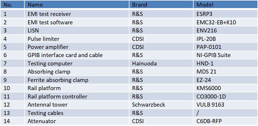
An engineer usually has to rely on his experience and on best practice methods in order to design an EMC compliant product. In order to show that a product complies with the essential requirements, the manufacturer is required to complete an EMC assessment which provides a record of a technical analysis justifying compliance. Nevertheless, it is estimated that >50% of products fail testing first time around. Failing is very expensive. Not only that re-testing costs are high, but also the project schedule and market introduction get delayed. Besides applying best practice with respect to all EMC related aspects of the design, it is essential to carry out pre-compliance testing, either in a test house or in-house. Pre-compliance in a test house is very expensive and time consuming. A test house is not always around the corner and not any time available; quick modifications of the product cannot be carried out as conveniently as in the own lab. Whereas pre-compliance in-house is convenient that modifications can be checked with respect to their effect on EMC immediately. Salom made a significant research investment in an internal EMC pre-compliance lab comprising a 3m compact anechoic chamber and a shield chamber. Main equipment as follows:

The lab could run pre-compliance testing against CISPR22, EN55022, CISPR14-1 and EN55014-1. Test capability including:
conducted disturbance at mains terminals between 150kHz-30MHz;
disturbance power between 30MHz-300MHz;
radiated disturbance between 30MHz-1GHz.
Conducted Disturbance at Mains Terminals

Disturbance Power

Radiated Disturbance

Further advice
The actual requirements for power supply product under the EMC standards can be complex and dependent on not only the design but also the type of user, the intended use and sometimes even what is claimed in the instructions or sales literature. Salom has a 40+ year history in the design and manufacture of power supply products that meet the most stringent EMC requirement. We have extensive experience of applying the requirements of EMC standards in all areas of the power supply industry including design, test and manufacturing and have received ISO-13485 certification for the manufacture of medical devices. We also continue to monitor the latest regulations to ensure full compliance in each region where our products are designed to be sold. We are a power partner of choice for many global brands. For further advice specific to your products, please contact us and we will be pleased to discuss your power needs.
*At least 1,400 'killed by NHS equipment failures':
http://www.mirror.co.uk/news/uk-news/least-1400-killed-nhs-equipment-3909340
*Medical Device Accidents: Recognition and Investigation